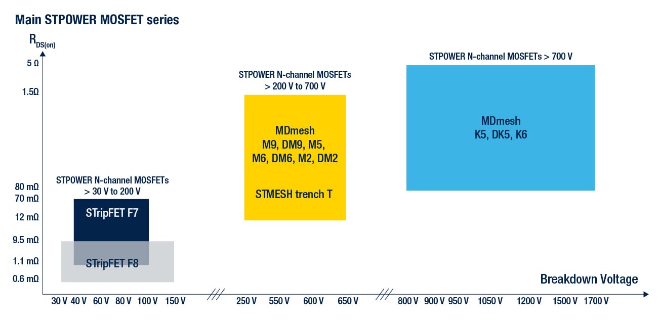
 意法半导体功率MOSFET产品采用先进的封装,具有很宽的击穿电压范围(-100到1700 V)、低栅极电荷和低导通电阻。我们通过面向高压功率MOSFET(MDmesh和STMESH沟槽)和低压功率MOSFET (STripFET) 的制程增强了功率处理能力,从而实现了高效解决方案。




产品类型
对于任意电压范围的工业和汽车应用(例如开关模式电源 (SMPS) 、照明、电机控制、能源生产和电动车辆、底盘与安全、车身与便利性等方面),意法半导体都能提供合适的功率MOSFET。
了解我们的产品组合
优势
- -100至1700 V击穿电压范围
- 面向低压到超高压功率MOSFET提供30多种封装选项,包括:
- 突破性的顶部冷却式HU3PAK封装,可实现更高的功率密度和更完善的热管理
- 4引线TO-247封装具有专用控制引脚,用于提高开关效率
- H2PAK封装,面向大电流能力应用
- 高度创新的表面贴装式无引线TO-LL封装
- 1 mm高的表面贴装式PowerFLAT系列 (2x2- 8x8 mm),带有大片裸露金属作为漏垫,使其具有优异的散热能力
- 改善了栅极电荷,降低了通态电阻,满足了当今极具挑战性的效率要求
- 面向特定产品线的本征快速体二极管
- 广泛的车规级功率MOSFET产品组合
- 面向应用的技术
Featured Videos


特别推荐
Automotive MOSFETs in tiny 5x6 mm dual-side cooling package
意法半导体扩大了AEC-Q101 MOSFET的产品范围,推出了两款采用先进的PowerFLAT™ 5x6双侧冷却 (DSC) 封装的40V器件,表面可湿。STLD200N4F6AG和STLD125N4F6AG的最大导通电阻分别为1.5 mΩ和3.0 mΩ,可确保较高效率并有助于简化系统热管理。0.8 mm厚的PowerFLAT 5x6 DSC保留了标准表面可湿封装的占位面积和热效率底部设计,同时使顶部源电极外露,以进一步增强散热性。此配置可达到更高的额定电流,从而提高功率密度,使设计人员能够在不牺牲功能、性能或可靠性的情况下构建更小的ECU。
Power MOSFET Basics
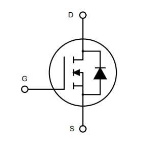
MOSFET stands for Metal Oxide Semiconductor Field Effect Transistor. It's a voltage controlled device with 3 terminals:
- Gate (electrically insulated from the semiconductor)
- Drain
- Source
When a voltage applied between the Gate and the Source reaches a certain threshold (VGS(th) or threshold G-S voltage), the device is able to support current conduction between the Drain and the Source (ID or drain current).
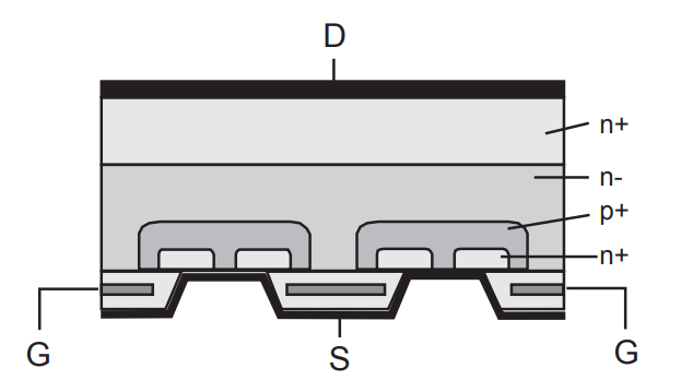
When a voltage applied between the Gate and the Source is below VGS(th), the device will withstand a voltage up to BVDSS (or breakdown voltage).
MOSFETs can be used as a signal amplifier (linear operation) or as a switch in power applications.
MOSFET parameters
Like many other types of semiconductor power switches, the main parameters of a MOSFET, usually available in most datasheets, are:
- RDS(on) (on-state resistance): electrical resistance when the device is set in on state. The lower is RDS(on), the lower is the conduction loss due to power dissipation when the current is flowing.
- BVDSS (breakdown voltage): maximum drain-to-source voltage that the device is able to sustain when in off state.
- QG (total gate charge): amount of electric charge required to the gate driver to turn on/off the device itself. QG impacts directly the efficiency (the lower, the better).
The product of RDS(on) and QG is known as the MOSFET Figure of Merit (FOM).
Other important parameters are intrinsic capacitances that can affect the switching times and voltage spikes, and body drain diode when device is used as power diode, like in synchronous free-wheeling operation mode.
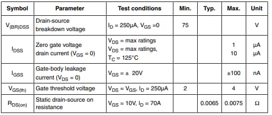
Learn more about how to read MOSFET datasheet parameters thanks to our series of videos dedicated to "Power MOSFET datasheet parameters".
Main types of power MOSFETs
MOSFETs can be of different types, including:
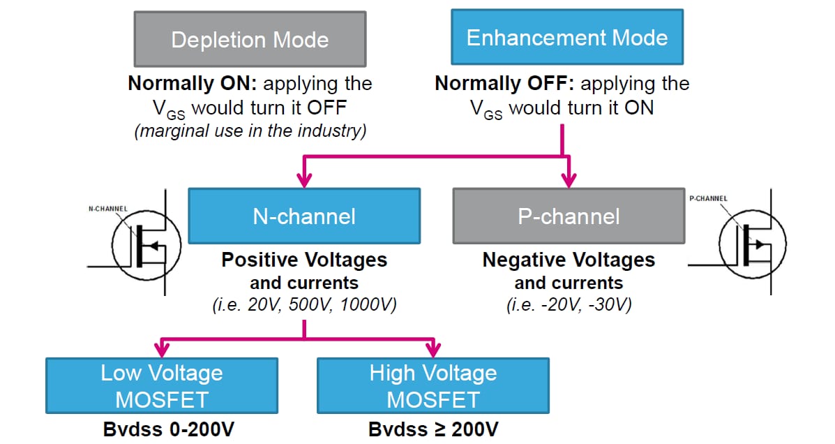
- Depletion Mode: Normally ON. Applying the VGS would turn it OFF.
- Enhancement Mode: Normally OFF. Applying the VGS would turn it ON.
- N-channel MOSFETs: positive voltages and currents.
- P-channel MOSFETs: negative voltages and currents.
- Low voltage MOSFETs: BVDSS from 0 V to 200 V.
- High voltage MOSFETs: BVDSS greather than 200 V.
N-channel enhancement-mode MOSFETs are the most popular type used in power switching circuits because of their low RDS(on) (on-state resistance) compared to P-channel MOSFETs.
Power MOSFET Applications
Power MOSFETs play an important role in all applications handling Power.
The main applications of high voltage MOSFETs include:
- Switch Mode Power Supplies (SMPS)
- Residential, commercial, architectural and street lighting
- DC-DC converters
- Motor control
- Automotive applications
ST's high voltage MOSFET portfolio offers a broad range of breakdown voltages up to 1700 V, with low gate charge and low on-resistance, combined with state-of-the-art packaging. ST's MDmesh™ high-voltage MOSFETs technology has enhanced power-handling capability, resulting in high-efficiency solutions.
The main applications of low voltage MOSFETs include:
- Switch, buck and synchronous rectification
- Uninterruptible Power Supplies (UPS)
- Small motor control
- Switch Mode Power Supplies (SMPS)
- Power-Over-Ethernet (PoE)
- Solar inverters
- Automotive applications
ST's low voltage MOSFET portfolio offers a broad range of breakdown voltages from -100 V to 120 V, with low gate charge and low on-resistance, combined with state-of-the art packaging.
eDesignSuite
eDesignSuite 是一套全面且易于使用的设计辅助工具,旨在帮助您简化系统开发过程,并支持广泛的ST产品。


电源管理设计中心
组件的热电模拟器
信号调节设计工具
NFC/RFID计算器
电源管理设计中心

电源设计工具
电源管理设计中心

LED照明设计工具
电源管理设计中心

数字电源工作台
电源管理设计中心

电源树设计器
组件的热电模拟器

STPOWER Studio
组件的热电模拟器

PCB Thermal Simulator
组件的热电模拟器

AC开关模拟器
组件的热电模拟器

整流二极管模拟器
组件的热电模拟器

Twister Sim
组件的热电模拟器

TVS模拟器
组件的热电模拟器

Estimate
信号调节设计工具

有源滤波器
信号调节设计工具

比较器
信号调节设计工具

低侧电流检测
信号调节设计工具

高侧电流检测
NFC/RFID计算器

NFC电感
NFC/RFID计算器

UHF链路预算
NFC/RFID计算器
