标准串行EEPROM让任何应用都更智能、更可靠。该产品组合提供高达400万次的写入/擦除循环和200年的数据保存时间。
这些非易失性存储器基于先进的110 nm工艺打造,属于低功耗解决方案,是提升应用性能的理想之选。
应用
.jpg)


.jpg)
产品类型
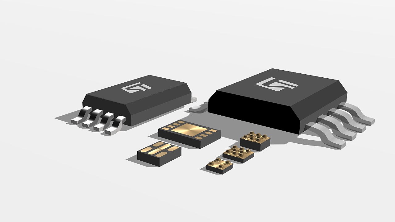
该产品组合包括SPI、I²C和Microwire等多种选择,并提供多种封装选项:SO8N、TSSOP8、DFN8、DFN5、WLCSP和裸片。
.jpg)
该产品组合的密度范围从1 Kb到4 Mb,工作电压范围为1.7 V至5.5 V。
该产品组合的密度范围从1 Kb到2 Mb,工作电压范围为1.6 V至5.5 V。
该产品组合的密度范围从1 Kb到16 Kb,工作电压范围为2.5 V至5.5 V。
优势
- 最高4 Mb
- 4 ms写入时间
- 85°C时低至1.6 V
- 105°C时低至1.7 V
- 低功耗
- 400万次写入/擦除循环
- 锁定页
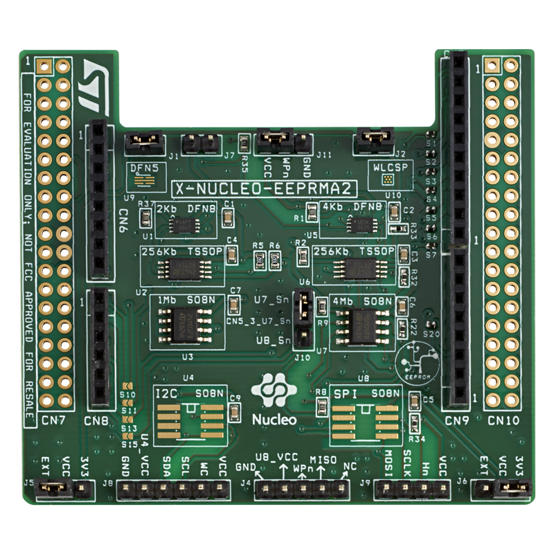
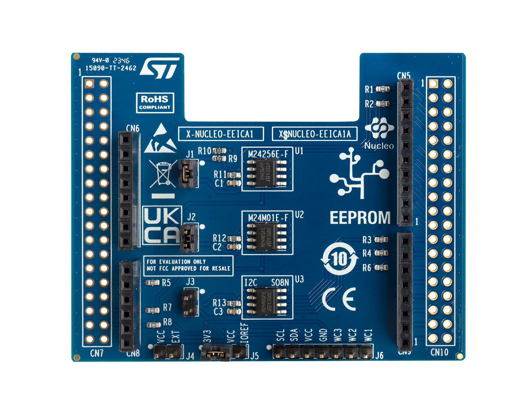
面向标准串行EEPROM的开发工具


I2C EEPROM(采用DFN5封装)的优点
4-ball WLCSP EEPROM designed for tiny Camera modules.
Camera modules for mobile devices follow a path of quick miniaturization while display resolution increases and requires a higher set of parameters to operate efficiently.
The 4-ball WLCSP I2C EEPROM family provides a minimal pin count, footprint and thickness, fitting the most stringent hardware design requirements. In addition, thanks to internally-wired device select code options, the EEPROM for rear and front cameras can share the same I2C bus, providing further module design optimization.
The factory-programmed settings can also be protected when selecting products with the software write-protect instruction.
Manufacturing robustness aspects are also covered with an optional back-side coating.
Choose your product: Compatible 4-ball I2C (with industry-standard footprint) or SWP 4-ball I2C (with software write-protect option)