产品概述
描述
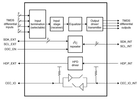
The STDVE001A integrates a 4-channel 3.4 Gbps TMDS equalizer. High-speed data paths and flow-through pinout minimize the internal device jitter and simplify the board layout.
The equalizer overcomes the intersymbol interference (ISI) jitter effects from lossy cables. The buffer/driver on the output can drive the TMDS output signals over long distances. In addition to this, STDVE001A integrates the 50 Ω termination resistor on all the input channels to improve performance and reduce board space. The device can be placed in a low-power mode by disabling the output current drivers. The STDVE001A is ideal for advanced TV and STB applications supporting HDMI/DVI standard. The differential signal from the HDMI/DVI ports can be routed through the STDVE001A to guarantee good signal quality at the HDMI receiver. Designed for very low skew, jitter and low I/O capacitance, the switch preserves the signal integrity to pass the stringent HDMI compliance requirements.
-
所有功能
- Compatible with the high-definition multimedia interface (HDMI) v1.3 digital interface
- Conforms to the transition minimized differential signaling (TMDS) voltage standard on input and output channels
- 340 MHz maximum clock speed operation supports all video formats with deep color at maximum refresh rates
- 3.4 Gbps data rate per channel
- Fully automatic adaptive equalizer for cables lengths up to 25 m
- Single supply VCC: 3.135 to 3.465 V
- ESD: > ± 5 KV HBM for all TMDS I/Os
- Integrated open-drain I2C buffer for display data channel (DDC)
- 5.3 V tolerant DDC and HPD I/Os
- Lock-up free operation of I2C bus
- 0 to 400 kHz clock frequency for I2C bus
- Low capacitance of all the channels
- Equalizer regenerates the incoming attenuated TMDS signal
- Buffer drives the TMDS outputs over long PCB track lengths
- Low output skew and jitter
- Tight input thresholds reduce bit error rates
- On-chip selectable 50 Ω input termination
- Low ground bounce
- Data and control inputs provide undershoot clamp diode
- Demonstration kit is available
电路原理图
EDA符号、封装和3D模型
意法半导体 - STDVE001A
Speed up your design by downloading all the EDA symbols, footprints and 3D models for your application. You have access to a large number of CAD formats to fit with your design toolchain.
Please select one model supplier :

符号

封装

3D模型