Product overview
描述
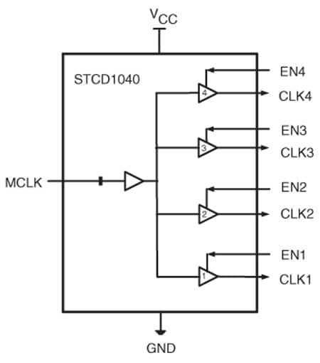
The STCD1020, STCD1030 and STCD1040 are 2, 3 or 4 outputs unity gain clock distribution circuits, which are used to provide a common frequency clock to multimode mobile RF applications. It can also be used for those baseband peripheral applications in a mobile phone such as WLAN, Bluetooth, GPS and DVB-H as a clock reference. The STCD1020, STCD1030 and STCD1040 isolate each device driven by their clock outputs and minimize interference between the devices. Each of the clock buffers can be disabled to lower the power consumption if the connected device does not need the clock. The STCD1020, STCD1030 and STCD1040 accept commonly used mobile master clock frequencies ranging from 10 MHz to 52 MHz.
The STCD1020, STCD1030 and STCD1040 are available in 2 mm x 2 mm 8-lead, 2 mm x 2.5 mm 10-lead and 2 mm x 3 mm 12-lead TDFN packages and can be operated with a single 2.8 V (or 1.8 V) supply. The operating temperature is 40 °C to +85 °C.
-
All features
- Operating temperature : –40 °C to 85 °C
- Available in TDFN packages
STCD1020 - 8-lead (2 mm x 2 mm) STCD1030 - 10-lead (2 mm x 2.5 mm) STCD1040 - 12-lead (2 mm x 3 mm) - 2.5 V to 3.6 V supply voltage
- Ultra-low phase noise and standby current
- 2, 3 or 4 outputs buffered clock distribution
- Individual clock enable for each output
- Single-ended sine wave or square wave clock input and output
- No AC coupling capacitor needed at the input
- 10 pF typical load driving capability
- Lower fan-out on clock source
电路原理图
EDA Symbols, Footprints and 3D Models
STMicroelectronics - STCD1040
Speed up your design by downloading all the EDA symbols, footprints and 3D models for your application. You have access to a large number of CAD formats to fit with your design toolchain.
Please select one model supplier :
Symbols
Footprints

3D models